TM 11-6625-1683-15, C9
the actuating pulse from the power converter
edge. This pulse is used to control Z2, which
reverses its direction and reaches the thres-
is a one-shot multivibrator that provides a 2 -
hold value of 2.5 volts dc, when the circuit
microsecond (usec) pulse.
is restored to its original state. This cycle of
b. The 2-usec pulse is fed to driver amplifier
operation occurs repetitively every 250 usec (B,
23 (fig. 9-11
which permits effective cou-
pling of the pulse into a low-impedance circuit
such as the block 500 gate generator. The trig-
gering pulse also appears at connector pins
of one-shot multivibrator Z2 (fig, 55) is to
J83, J20-3, J222, and J24-H.
maintain the rectangular waveform created
by squaring amplifier Z1 for a specific dura-
tion. Since the waveform width developed in
the squaring amplifier is governed by the time
(approximately 0.5 usec) required by the sync
p u l s e to rise through and then fall back
through the threshold level of 2.5 volts dc,
the one-shot multivibrator serves to extend the
wave duration to approximately 2 usec. Op-
erationally, the positive-going leading edge of
the output signal produced by squaring ampli-
fier Z1 is coupled to the base of input transis-
tor Ql, which is normally biased into a con-
ductive state, The impressed signal alters this
state, and Q1 is driven into nonconduction.
T h i s permits the base of transistor Q2 to
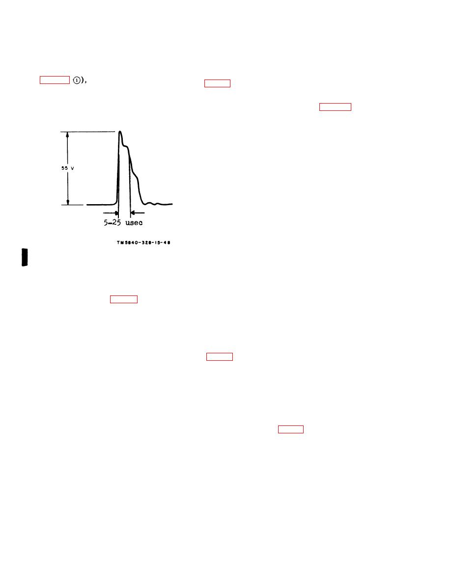
Figure 52. SYNC pulse waveshape.
become more negative, and, consequently, Q2
swings into conduction. However, during the
5-8. Triggering Circuit
period of nonconduction, capacitor C2 acquires
a charge that holds the circuits in its acti-
a. Squaring Amplifier Z1. The function of
vated cycle, even after the decay of the actuat-
squaring amplifier Z1 (fig. 54) is to translate
the asymmetric synchronized (sync ) pulses
ing signal. This condition is sustained until
developed by the receiver-transmitter power
capacitor C2 is discharged, at which time the
c o n v e r t e r (block 700) into well defined,
circuits are restored to their quiescent state.
sharply rising pulses with uniform amplitude
The component values are selected to provide
and a rectangular-shaped
w a v e f o r m . To
a time constant of approximately 2 usec (C,
accomplish this, a modified Schmitt trigger
circuit is employed. In operation, no output
c. Driver Amplifier Z3. To provide a trig-
signal occurs until a positive-going pulse is
applied to the input. When the input signal
gering signal to external circuits without in-
exceeds a predetermined threshold level (2.5
troducing variable loading conditions on the
v o l t s dc), i n p u t transistor Q1 switches
one-shot multivibrator, with consequent de-
abruptly from the conductive to the noncon-
viations in operating characteristics, it is es-
ductive state. With the voltage at the collec-
sential that a decoupling system be employed.
tor of Q1 at the nonconductive level, the bias
Driver amplifier 23 (fig. 56) serves this pur-
on the base of output transistor Q2 is shifted
pose. It consists of a twin, two-stage ampli-
in the negative direction, causing Q2 to be-
fier with inputs and outputs, each connected
come conductive. As a result, the normally
together to provide paralleled circuits. The
negative polarization of the collector shifts to
frequency response characteristic permits op-
a zero potential. This condition prevails until
eration from 0 to 50 kHz, which enables the
5-4


 Previous Page
