TM 11-6625-1683-15
TM5840-328-15-53
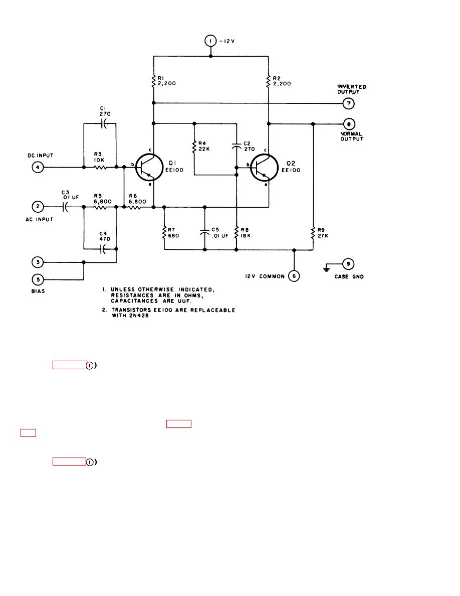
Figure 54. Squaring amplifier 21, schematic diagram.
radar set. Through this connector, power and
5-9. 400 CPS Output Circuit
circuit connections are established. RCVR
GAIN potentiometer R7 controls the gain of
Test jack TP60 (white) and test jack TP61
the intermediate frequency (if.) preamplifier
(black) permit observation of the 400Hz sig-
located on the tr assembly. AFC GAIN poten-
nal that appears at connector J11 in block
tiometer R8 provides control of the gain of
2400, connector J12 in block 2800, and con-
the afc preamplifier located on the tr assem-
nector J14 in block 1000. Waveforms developed
bly. ON/OFF switch S6 is a three-pole, two
in the triggering circuit are shown in figure
p o s i t i o n toggle switch that controls the
power delivery to connector J7. In the ON po-
sition, one pole supplies 5 volts to pin J7-C,
5-10. Block 100 Tr Assembly Test Circuit
the second pole supplies + 6 volts to pin J7-B,
and the third pole furnishes + 110 volts to
Connector J7 provides a means of intercon-
pin J7-J. In the OFF position, these power
nection with the block 100 tr assembly of the
circuits operate, respectively, into dummy load
5-6
AGO 7918A


 Previous Page
