
TM 11-6625-1683-15
TMS840-328-15-55
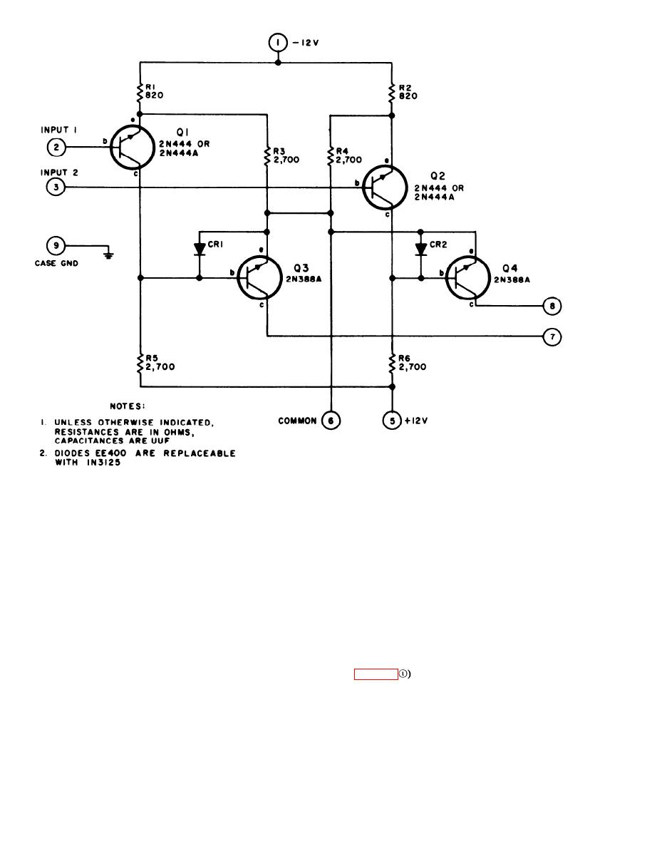
Figure 5-6. Driver amplifier Z3, schematic diagram.
Resistors R2, R1, and R3. OSC CUR test jack TP1l
b. In the OFF position, these power circuits feed,
enables monitoring of the local oscillator current in
respectively, into dummy load resistors R5, R6,
the tr assembly or the 7-volt dc output of the SSLO
and R4. RCVR-XMTR VIDEO test jack TP2
voltage regulator. On some test panels, AC test
permits monitoring the video output from the if.
jacks provide connection to measure 6-volt ac
amplifier to the receiver-transmitter headphone
output of block 700 power converter.
circuits, and CONT -- IND VIDEO test jack TP3
provides a monitoring point for the video output to
5-11. Block 300 If. Amplifier Test Circuit
the control-indicator.
a. Connector J4 provides a means of intercon-
nection with the block 300 if. amplifier of the radar
5-12. Block 400 Boxcar and Audio Amplifier
set. Through this connector, power and circuit
Test Circuit
connections are established. ON/OFF switch S2 is
a three-pole, two-position toggle switch that con-
trols the power delivery to connector J4. In the ON
a. Connector J6 provides a means of interconnec-
position, one pole supplies 5 volts to pin J4-C, the
tion with the radar set block 400 boxcar and audio
second pole supplies +12 volts to pin J4-H, and the
amplifier. Through this connector, power and
third pole furnishes +6 volts to pin J4-B.
circuit connections are estab-
Change 10 5-8

 Previous Page
